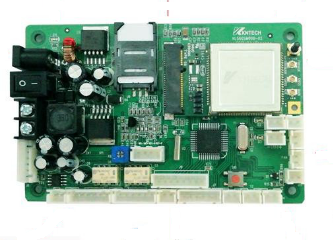
PCB customer data analysis:
The basics of PCB Board Factory manufacturing a multi-layer printed circuit board, or PCB for short. During the quotation stage, the customer’s data is checked against capability after order acceptance, and the contract review is undertaken, which checks data drawings assumptions and laminate availability. The customer’s data, ODB Plus+ or Gerber, will automatically be checked against our capability if alterations are required. The customer will be contacted by EQ from the single customer circuit and will be stepped up to fill the production panel 24 by 18 or 18 by 16.
The chemical solutions present in the PCB Board Factory production lines are regularly analyzed to ensure they meet the stringent levels determined by the suppliers of the Process. The laminate and prequel specified on the route card are pulled from stock, checked for compliance, and released to production; the batch codes are recorded on a build sheet. So material traceability to the source can be maintained; the C a.m. image is transferred onto the circuit by laminating The inner layer material with UV-sensitive photosensitive resist.
The inner layers are Auto loaded onto the cleaning line passing through a chemical edge dryer for removal and preheating before having the dry film resist applied to the laminate using heat and pressure the resist is then exposed to UV light in specific areas, which polymerizes or hardens the film to create the circuit Image. The exposure can be achieved using either artwork and UV light or a direct imaging machine that uses a laser to scan the CA n image onto the UV-sensitive resist.
PCB Board Outer layers :
The outer layers are also printed similarly, except that the outer image is reversed. This PCB Board Factory process is completed before the panels are run through the pattern plate line the DES machine is standing for developing edge strip; firstly, the operator removes the protective Milo coating before loading it into the developer section of the DES. This removes any resist that hasn’t been exposed to UV light; the board then passes through the etch stage, which chemically removes the copper. Finally, the mask that has been UV cured and has stopped the etch from attacking the copper is removed in the stripping section of the line; the manufacturing data from the CA M. its compared against the circuitry on the panel using the automated optical inspection machine the panel is cleaned before scanning the Layer. The Aoi scans the circuit board and highlights differences from the CA m data. Any discrepancies are checked by the operator and either repaired or discarded using the appropriate IPC Rules.
The panel is treated using a chemical edge which Ruffins the surface of the copper to a dad, even giving the copper a salmon pink appearance. The inner layer panels are stacked up with prepreg, a glass fiber sheet impregnated with resin between the layer pears, and copper foil placed outside the stack. The required order shown on the build sheet pressure and heat is applied under a vacuum at specific parameters, which allows the resin in the prepreg to flow and bond. The layers at this stage drill the holes that will form the electrical connections between the layers of the PCB. The locations are determined by the customer’s design to fit specific components; drilled hole sizes are usually 100 micrometers larger than the finished hole sizes to allow for the copper plating process. The drill machine can detect when the drill piece has a broken or chipped drill, and when the job becomes blunt can automatically change to new drill panels. It can be drilled up to four high depending on board thickness, drill size, and copper content; after this stage, a thin coating of copper is chemically deposited on all the exposed surfaces of the panel. That includes the whole walls; this creates a metallic base for electroplating copper into the holes and onto the surface.